DC To DC Converter Circuit Diagram With IC 555
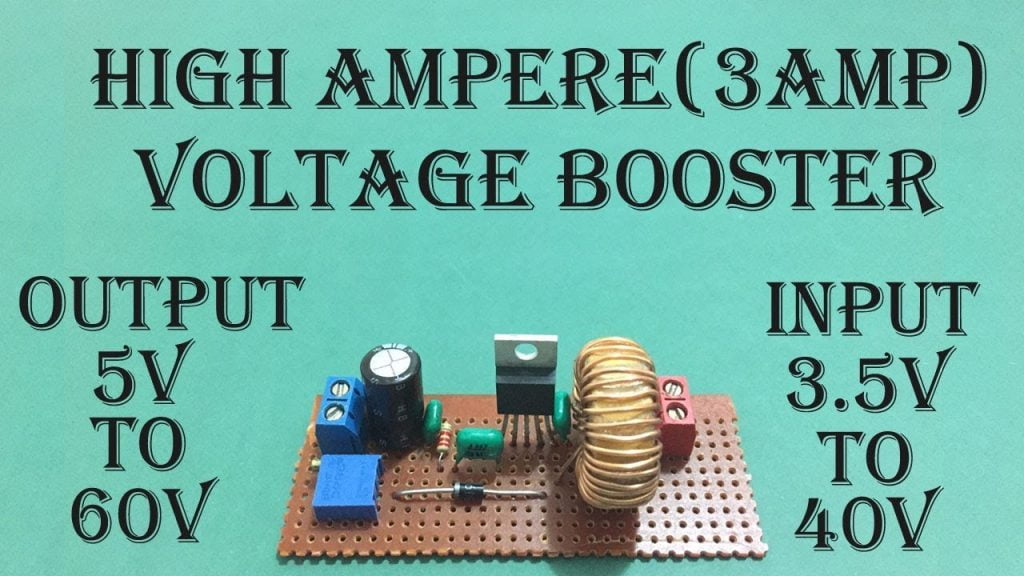
In this article, we design a dc to dc converter circuit diagram with ic 555 and MOSFET that can supply high voltage at the Output than its Input. This boost converter circuit operates from 5V to 12V and can generate variable voltages up to 50V. Let’s know how Voltage Booster circuit works. Everything is explained in this article with the help of video
What is a Voltage Booster Circuit
Voltage Booster Circuit is a dc to dc voltage converter that always has a higher output voltage than input and a lower output current than input. This is a class of switching power supplies (SMPS) that can efficiently convert voltage from one level to another, ideally with equal input and output power.
The main circuit of a practical voltage booster consists of two semiconductors and two energy storage components. The two semiconductor components are a MOSFET switch and a Schottky diode. The two energy storage components are an inductor, which plays an important role in boosting the voltage, and a capacitor used to smooth the DC output.
DC To DC Converter Circuit Diagram
This circuit is made from easliy available components. The above circuit consists of two stages: the oscillator and boosting stage let’s explore them in detail.

Parts List of DC To DC Converter, Voltage Booster Circuit
- Ic 555 must be CMOS type other wise NE555 TTL ic will not work at 5v vdc
- Inductor 50uh-100uh 3amp or as per your Load
- Diode D1 & D2 1N414, D3 1N5822, D3
The recommended diode is 1N5822 which is a fast switching schottky diode designed to operate at higher frequencies like this and also it has a lower forward drop voltage which contributes to greater efficiency.
You can also use a silicon diode 1N4007 in case you don’t have a schottky diode, but there will be efficiency Losses.
- Capacitor C1 470, C2 104( Ceramic capacitor), C3 100uf to 1000uf/50 volt or above
- Mosfet Q1 IRLZ44, If you didn’t have an IRLZ44N MOSFET you can substitute with IRFZ44N MOSFET, the circuit still works, but there will some efficiency losses.
- Resistor R1 1k, R2 4.7k both 1/4watt(quarter watt)
- Variable Resistor VR 50k
It requires only a few external components. The IC consists of many good features and functions. Built inside its circuitry which are, built-in 3A NPN switch at output, 52 kHz oscillator, current limit function, automatic overheat shutdown, automatic over-voltage shutdown etc. Read More…
How This DC To DC Voltage Booster Circuit Works
Before working of the circuit , you need to know about its Main components
- Inductor:- Inductor opposes sudden/fast changes in the current. It can store energy in the form of a magnetic field. When the stored magnetic field collapses on the inductor (when the source is removed) the polarity of generated current across the inductor is opposite to what the source used to build its magnetic field.
- IC 555:- The evergreen IC 555 is configured in astable multivibrator mode, which oscillates at around 30 KHz with the help of RC components connect around it. To control the output voltage we need to control IC 555’s duty cycle, to accomplish this two fast switching diodes 1N4148 are connected anti-parallel between pin #7 and a 47K potentiometer, by rotating the potentiometer clock and anti-clockwise we can adjust its duty cycle and so does boost converter’s output voltage.
- Role of 4.7k Resistor:- A 4.7K resistor is connect to 47K potentiometer’s output terminal to limit the IC 555’s duty cycle to 90%, this is very important because if a user rotates the knob fully, the output will get saturated i.e. 100% duty cycle.
At 100% duty-cycle the MOSFET is ON continuously and creates full short circuit via inductor.
We also found using simulation that approximately above 90% duty-cycle the output voltage did not raise but reduced significantly, this could be because the MOSFET is ON for too long and not enough time for the inductor’s magnetic field to collapse and generate a voltage across it.
-
Mosfet:-The recommended MOSFET for this boost converter is IRLZ44N (not to be confused with IRFZ44N), IRLZ44N is a logic level MOSFET which can fully turn ON at 5V (Vgs), we need such lower GATE voltage because as a boost converter circuit we’ll be applying a lower voltage like 5V/6V to extract a higher voltage from it, at these lower voltages other general purpose MOSFET won’t fully turn ON.
If you didn’t have an IRLZ44N MOSFET you can substitute with IRFZ44N MOSFET, the circuit still works, but there will some efficiency losses.
-
Diode:-
The booster circuit has a schottky diode which prevents the charge stored in capacitor flowing back to inductor and ensures the boosted voltage passes to electrolytic capacitor and load.
The recommended diode is 1N5822 which is a fast switching schottky diode designed to operate at higher frequencies like this and also it has a lower forward drop voltage which contributes to greater efficiency.
You can also use a silicon diode 1N4007 in case you don’t have a schottky diode, but there will be efficiency losses.
-
Capacitor:- We are using a standard electrolytic capacitor with voltage rating of at-least 50V; this is because the proposed boost converter circuit at no load condition can shoot well above a pre-set voltage and the capacitor needs to withstand it.
How This Dc To DC Converter Circuit Works
The working of boost converter can be understood better using two scenarios:
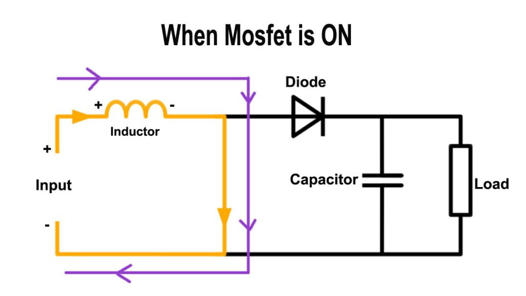
- When the MOSFET is ON.
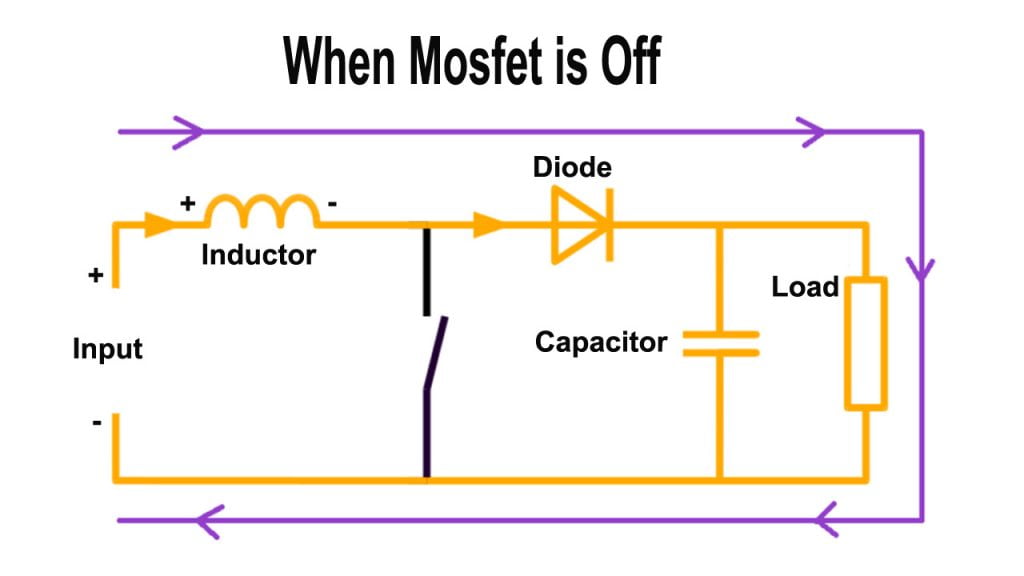
- When the MOSFET is OFF.

When Mosfet is ON
- When the MOSFET is ON, current passes through the inductor, through the MOSFET and finally to the ground.
- As mentioned earlier the inductor does not allow sudden changes in the current, meaning when the MOSFET is ON inductor won’t allow full current from the input to pass through the MOSFET and to the GND, instead the current will rise slowly in micro-second time frame.
- The slow rise in the current is due to the inductor converting the current in to magnetic field around it. Once the magnetic is fully built around it there will be no opposing in the current flow (the MOSFET will be turned OFF before the inductor fully built its magnetic field, because it will cause short circuit).
- When the inductor has built sufficient magnetic field around it in the above shown electrical polarity the MOSFET will be turned OFF. Let’s continue understand what happens when MOSFET is turned OFF.

When Mosfet is OFF
- When the MOSFET is turned OFF fully, the inductor can no longer support its magnetic field around it, so it collapses on the inductor itself and act as a DC generator in the above shown electrical polarity (which is opposite to what the input supply built its magnetic field).
- Now if you take a look at the above circuit, you will observe that the generated voltage across the inductor is in series with the input voltage, these two voltages add-up like when two cells connected in series, now the output will be sum of the two voltages.
- This higher voltage is passed through a diode and charges an electrolytic capacitor. The diode prevents the charge flowing backward and ensures the stored charge is passed to a load connect at the output.
- The MOSFET is turned ON again before the capacitor loses any significant amount of charge to maintain a steady voltage across output.
PCB Layout For DC To Dc Voltage Booster Circuit
Please Watch Video How to make PCB For this Circuit or download gerber file form above link


