What is the PCB (Printed Circuit Boards) Fabrication Process?
Introduction to PCB Fabrication: PCBs (printed circuit boards) play a significant role as components in electronic devices. PCBs are used to connect electronic devices via conductive channels. The PCB fabrication process creates these boards from scratch, to ensure accuracy and reliability in the production of electronic equipment.
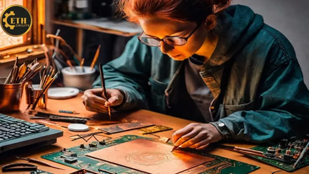
Designing the PCB Layout: To start the creation process of PCBs, designers focus on creating a diagrammatic plan that gives the outline of connections and components. The use of designing software of PCB boosts this process and also helps with the efficient placement of components and routing. Before moving forward, it is important to verify the functionality of the layout via prototyping and testing.
Creating the PCB Prototype: It is critical to select suitable materials before manufacturing the physical PCB. To define the conductive pathways, the designer etches the copper layer. Subsequently, drilling and finishing steps ensure the accuracy of component placement and board dimensions.
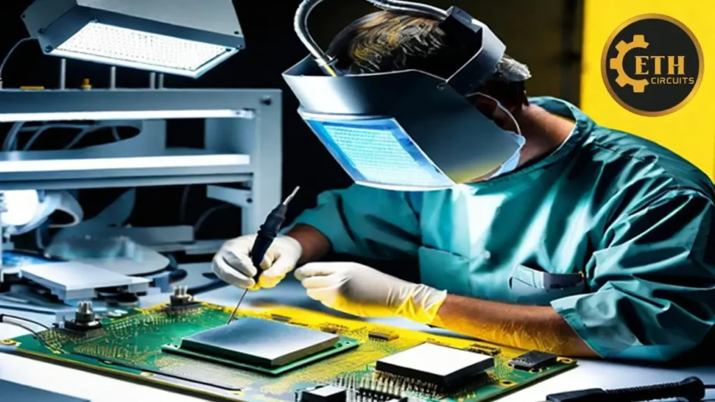
Fabricating the Final PCB: After a successful prototype, designers start applying solder masks and silkscreen layers. To ensure that the manufactured board meets industry standards they took quality control measures. Final testing of PCB confirms its reliability and functionality.
PCB Assembly: The black canvas of the circuit board is created by PCB fabrication and the circuit board is brought to life by PCB assembly. In this stage, electronic components are assembled and soldered onto the fabricated PCB. Companies like NextPCB offer high-quality PCB assembly services, ensuring accurate placement and robust connections for your electronic devices.
Summary: In this detailed guide, we have gone over the step-by-step fabrication process of PCB and explained involved in circuit board designing, prototyping, and fabricating. For enthusiasts or to become a professional in the electronics industry the understanding of these processes is essential.
FAQs
What materials are commonly used in PCB fabrication?
Common materials include FR-4 substrate, copper foil, solder mask, and silk screen.
2. How long does it typically take to fabricate a PCB?
The timeframe for PCB fabrication varies based on complexity but can range from a few days to a couple of weeks.
3. Are there any environmentally friendly PCB fabrication methods available?
Yes, some manufacturers are adopting eco-friendly practices such as water-based inks and lead-free soldering to reduce environmental impact.
Remember, the PCB fabricationprocess is a precise and detailed endeavor, requiring expertise and attention to detail at every stage. PCB fabrication also has the importance of PCB assembly in its process. By following this guide, you can gain insights into the world of PCB manufacturing and assembly, enhancing your understanding of this critical industry.